PCB Design Service

PCB Design & Layout Service

AUSPI can help you convert your ideation/schematic into a finished PCB ready for assembly.

Design your boards correctly from the start

We design printed circuit boards of any complexity: rigid, flexible, multilayer, HDI boards, high-speed PCBs, and other types.

Our team can create boards from scratch or improve an existing electric circuit design. We will create a prototype, develop embedded software, test the product, and prepare PCB design and layout documentation.

PCB designers at AUSPI have the experience to bring your boards to life.Whether you’re developing a new product or reverse engineering an existing one, we are an integrated part of the most dependable full-service PCB design and manufacturing team in the world.

Professional and Interactive design teams in Europe and China with average more than 8 years’ experience, and longest 15years+, specialized in ID, mechanical, electronic hardware, firmware and software, media etc, can design from concept to demo, and from demo to products. We use design soft Cadence、Altium、Pads、Protel etc, can design independently boards in industrial, medical, consumer, communication, fiber network electronics, covering high speed, high density, digital analog mix layout design. We are also experienced with multilayer boards with blind and buried vias.

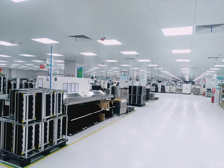
Schematic Diagram Design

Our team consists of experienced engineers, such as FPGA senior engineers, antenna experts ect. No matter how complicated the project is, our engineers can design the schematic diagram to meet your requirements.

3D Printing& Enclosure Design

Work with our team of 3D printing & Enclosure design experts to reinvent the way you produce jigs and fixtures, rapid prototypes, tooling, on-demand parts and low-volume production runs. Our powerful 3D printing & Enclosure technology that produces highly accurate and durable parts that are capable of being used directly in end-use.

PCB Design and Layout

We use different PCB design softwares to meet your needs: Altium Designer; Cadence Orcad or Allegro; Eagle; KiCAD

Algorithm Development

If you meet algorithm problem, we can help you solve it. Our algorithm engineer has rich experience in image processing, data processing and so on.

Electronics PCB Design & Re-Design & Reverse Engineering

Integra creates analog, digital, and mixed-signal boards for custom electronics.

As a PCB solution provider, we can provide consultation, evaluate your project, and offer a full cycle of development – from schematics and layout to testing and validation.

We use the DFMA approach in our work and can help you with certification and production launch.

industries pcba 1 1024x768

Industrial projects

We’re experienced with IPC, PLC, DCS, FCS, CNC including high power consumption X86, and low power consumption ARM framework. Framework ever handled including Haswell, Sandy bridge, Core, Bay trail

iot

Communication Products

Over 10years experiences designing in this industry, focusing high speed, complete of signal and power and whole design planning. Main console including FPGA, ARM, DSP, in field of CPCI, ATCA, VME, PXI. Experienced with fiber interface of SFP10G, high speed connector, high speed signal(3.125G 5G 6.25G 10G)

image 22 4

Consumer electronics

Experienced with HDI, Arm and Bluetooth, high frequency(2.4G,5G WIFI,GPS 3G,IQ), ESD based on IEC61000-4-2/GB17626.2

ccd e1670816563827 1024x683

Safety and camera

Experienced with EMC and complete of signals; Main control platform using Hisilicon, Ti; Applications of design in HD NVR, HD matrix.

components 1 1024x628

Automotive Electronics

Specializing in PCB design for automotive peripheral electronic devices. Designed products include in-car computers and dashcams. Designed main control platforms include Ambarella, Rockchip, Allwinner, and MediaTek. Product solution designs include rearview mirrors, single-lens, dual-lens, dual-channel coaxial cable, dual 1080P, and various other options.

pcb assembly

Seamless interaction with manufacturing

We cater to numerous electronics customers. We have cross industry experience in PCB design and work with current technologies for defense and space, medtech, automotive, telecommunications, etc. Thus, we are in a position often to provide insights into schematic designs and proactively give feedback on schematic errors and layout methods.

As we have our own PCB fab and assembly facilities in 5 continents, the benefits of working with us include seamless interaction with manufacturing, in-house stack-up design, component purchase, and material selection.

Output of a design

AUSPI optimizes your PCBs with full intellectual property protection and uses the most trusted design tools.

Trusted by Industry Leaders

Engineers at the world’s industry leading companies choose AUSPI for the highest quality PCB design support services, in multiple countries..

Testimonials

Design Layout Services

At the AUSPI design team, our designers address these challenges with a combination of adherence to the most current industry- standard design rules and the expertise developed over decades of design experience.

  • High Density Interconnect (HDI)
  • Signal/Power Integrity Design
  • Dense High-Speed Digital
  • RF and Rigid Flex

PCB design software capabilities

  • Altium Designer
  • Cadence OrCAD/Allegro
  • Eagle
  • KiCAD
  • Siemens EDA

Certifications

  • ISO 9001
  • ISO 16949
  • RoHS
  • CE/FCC

Cost optimization

We can review an existing product or design and propose methods for cost reduction. In many cases, layer reduction can be achieved by using smaller geometries for conductors and vias and the use of laser-drilled microvias.

PCB stack-up design

Before we start the layout design, we will do an in-house stackup design so that all the design objectives are met. We will also suggest if HDI technology is required or could help in PCB optimization.

Signal integrity services

We can perform signal integrity services on any high-speed board designs that we make. We will take care of control impedance and crosstalk requirements; we will take care of PCB materials that are suitable to achieve a given set of signal integrity specifications.

FAQs

General Lead times
  • From one week to 3 months depends on different projects
  • PCB layout one to two weeks
  • Schematic 1~3days
  • DEMO about 3days

Please, send us the following documents and information to get a prompt PCB design support quote:

  1. Schematic in PDF format
  2. Bill of material in Excel /csv format preferred
  3. Mechanical diagram of required board DXF file or PDF showing the dimensions of the board
  4. The maximum frequency on the board
  5. Block diagram, if from concept stage

We are now proud to offer design services that will support superior execution in fabrication.

  • Automotive
  • Lighting
  • Industrial
  • Medical
  • Computing
  • Telecommunications

Meet the AUSPI Global Service Network

AUSPI team locates in USA, MEXICO, San Paolo, Czech, Portugal, St. Peterburg, provides global competitive pricing and fast, accurate production quotes. Scale up and down quickly. We offer inventory management, integrated fulfillment, and system integration.

Start Your Design Quote Now!

HOW AUSPI HELP YOU ?

With over 20 years of experience, Auspi has firmly established itself as a leader in client satisfaction across diverse industries. Our strategically positioned facilities in the Americas, Europe, and Asia allow us to effectively meet both your geographical and cost requirements. We carefully balance quality and affordability, ensuring that every penny you invest delivers exceptional value.

In the fast-evolving and competitive electronics industry, we remain agile and innovative. By continuously expanding our service offerings, we ensure that we not only meet but exceed the expectations of our valued partners. Your success is our priority, and we are dedicated to staying at the cutting edge of industry advancements to support your growth.

image 3 5

01/ Reliability

  • Full Compliance with NDA Requirement;
  • Strictly Follow Customer’s Original Design;
  • Good Quality Performance & Keep Improving;
  • Honoring Our Commitments

02/ Expertise

  • Full Manufacturing Process Coverage;
  • Decades Focusing & Rich Experience;
  • Turn Key & One-Stop Solution
  • Components Sourcing & SCM

03/ Fast Response

  • 8 hours RFQ Reply & Online Chat
  • 24 Hours Feedback on Customer Complain
  • 72 Hours PCB Bear Board Sampling;
  • 2-3 Weeks PCBA Prototyping (TurnKey BoM)

04/ Flexibility & Quickturn

  • NO Minimum Order(MoQ) Requirement;
  • Wide Rage of Components Inventory;
  • Expedite Services;
  • Diversity, Equity & Inclusion

05/ Worldwide Supply

  • 8 Branches Worldwide; (see contact us)
  • 4 Manufacturing Bases Located in China, Czech Republic, Mexico & Malaysia;
  • Multi-sites Phone Access & Local Supporting

06/ Reasonable Cost

  • Transparent, BoM Cost Breakdown;
  • Live Stock and Pricing Data;
  • Alternative Scenarios Proposal
  • Competitive Pricing
Scroll to Top